4. Structure Modeling
Device Studio supports importing structures from local or online databases, or building new structures based on imported ones. It supports creating various molecules, crystals, and typical device structures such as LCR/LR/FCB/FB/BCT/BT. Device Studio can automatically split crystal planes and build device structures according to user-specified matching accuracy requirements. It can automatically match and build multilayer device or crystal structures. It can generate special structures such as Nanoribbons, Nanotubes, clusters, grain boundaries, and random doping.
Device Studio supports file types including .hzw, .xyz, .cif, .dsxml, .pdb, .mol, .xsd, scf.input, .py, POSCAR, CONTCAR, etc., where .hzw is Device Studio’s proprietary file format. Device Studio can export structure files in .hzw and .xyz formats according to user needs, and can export 3D visualization results of structure files in .png image format. For crystal structures, it can identify their space group structure information and export structure files in .cif format.
Before importing a structure, you need to create a new project or open an existing project, and import the structure based on an existing project. To create a project: double-click the Device Studio icon shortcut to log in and start the software. The graphical interface is shown in fig. 4.1. According to the interface prompts, select the button to create a new project ( Create a new Project ) or open an existing project ( Open an existing Project ), then click the OK button. If you choose to create a new project, you can name it according to your needs, such as naming this project Device Studio.
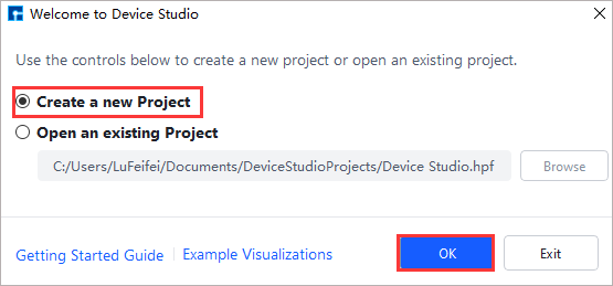
fig. 4.1 Graphical interface for selecting to create or open a project after starting the software
4.1. Importing Structures from Local Database
Device Studio comes with a local database containing over 500 commonly used or popular materials, which will be continuously updated and expanded. If users need a large-scale database, they can pay attention to Hongzhiwei’s FIRST software, which includes three major databases: QuickMol, QuickCrystal, and ACED, with over 10 million material entries. Users can import structures through the local database, such as importing the ZnO-MgO-Si device structure. The import operation is shown in the red part of fig. 4.2: File → Import → Import Local. Then a graphical interface pops up as shown in fig. 4.3. According to the interface prompts, find the folder containing ZnO-MgO-Si in the local database, select the ZnO-MgO-Si structure file, and click the open button in fig. 4.3 to import the ZnO-MgO-Si structure. The graphical interface after importing the ZnO-MgO-Si structure is shown in fig. 4.4, where the ZnO-MgO-Si.hzw structure file is in the Project Explorer area, and the 3D view of the structure is displayed in the 3D Viewer area.
Note
If you don’t want to import the structure through the database, and you know the location of the structure file, such as the ZnO-MgO-Si structure, you can simply left-click to select the structure file and drag it to the Project Explorer area of Device Studio to import the structure. The 3D view of the structure will be displayed in the 3D Viewer area.
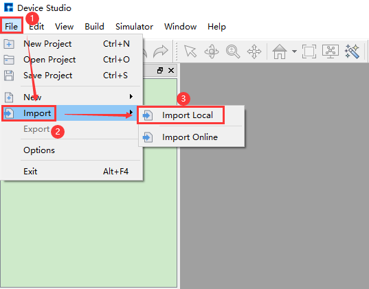
fig. 4.2 Pop-up interface for importing structure from local database
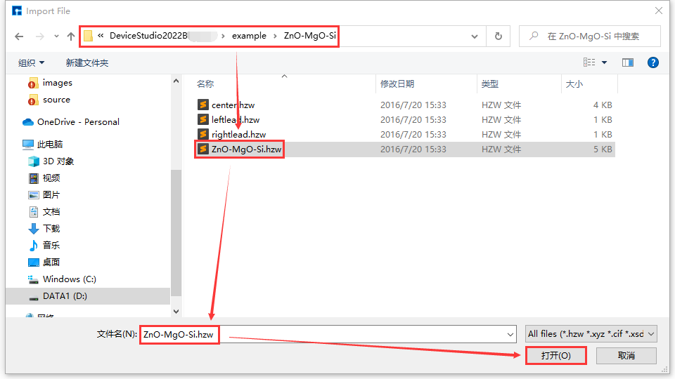
fig. 4.3 Interface for selecting ZnO-MgO-Si structure file
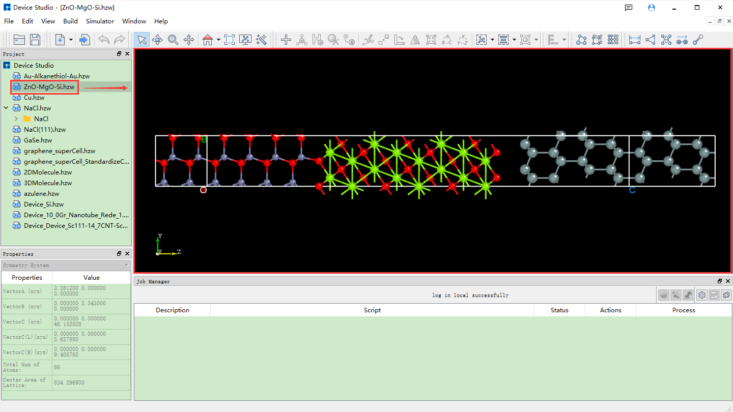
fig. 4.4 Device Studio interface after importing ZnO-MgO-Si structure
4.2. Importing Structures from Online Database
Device Studio supports connecting to the online Materials Project database. As shown in the red part of fig. 4.5: click File → Import → Import Online to pop up the interface for importing structures from the Materials Project database. In this interface, users can search for atomic structures by entering elements, chemical formulas, or mp numbers.
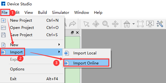
fig. 4.5 Pop-up interface for importing structure from online database
As shown in fig. 4.6, search for structures by entering elements. Enter the Si element and click the Search button or press the Enter key on the keyboard. Many atomic structures containing only Si elements will appear, such as the Si40 structure. The left side shows its detailed chemical formula, and the right side shows its corresponding space group structure. After selection, you can view the structure’s chemical formula, space group symmetry information, and atomic coordinates in the red box area at the bottom left of the interface. You can view the 3D display of the structure in the red box area at the bottom right of the interface. For the 3D display of the structure, you can zoom in or out by scrolling the mouse wheel. You can right-click to select the structure and rotate the 3D view by dragging the mouse. After determining the atomic structure to search for, click the Add button in the interface to import the atomic structure. The structure file is saved in the software’s project management area (Project Explorer), and you can view the 3D view of the atomic structure in the 3D display area. The Device Studio interface after importing the Si40 structure through the online Materials Project database is shown in fig. 4.7.

fig. 4.6 Materials Project element search and structure import operation interface
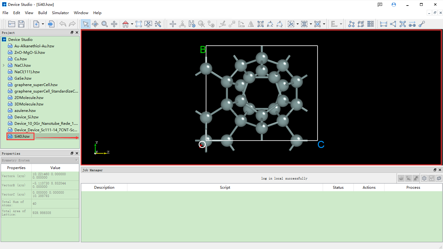
fig. 4.7 Device Studio interface after importing Si40 structure
The operations for searching and importing structures through chemical formulas and mp numbers are the same as those through element search and import. Their operation interfaces are shown in fig. 4.8 and fig. 4.9 respectively.
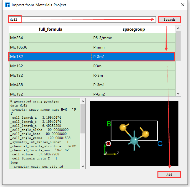
fig. 4.8 Materials Project chemical formula search and structure import operation interface
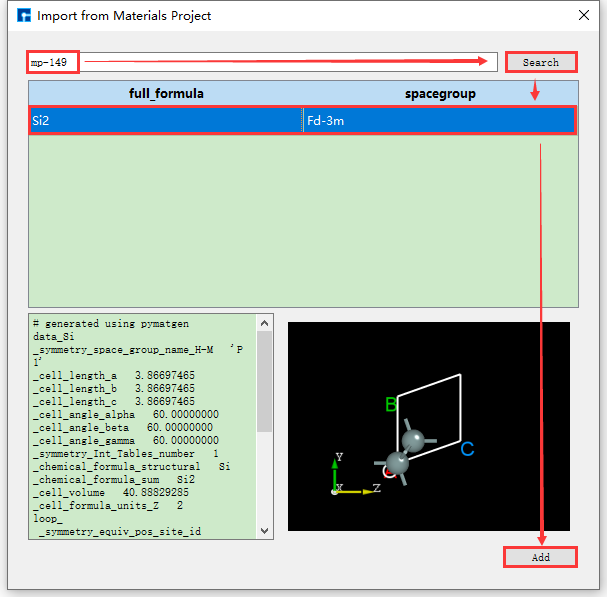
fig. 4.9 Materials Project mp number search and structure import operation interface
Device Studio 2022A version adds the 2D Molecular Modeling function. In the 2D molecular modeling interface, its toolbar contains various bonds and tools for drawing molecular structure formulas, including chemical bonds, ring templates, folded chains, boat structures, chair structures, arrows, borders, and text editing tools. Users can quickly and conveniently draw various 2D planar molecular structure formulas and write equations through this function, and it supports converting 2D molecular structures into 3D molecular structures.
Device Studio has the function of editing 2D molecular structures. Users can perform operations such as rotation, modifying bond width, bond length, bond position color, bond position type, bond position attribute conversion, adding hydrogen, removing hydrogen, adding charge, removing charge, etc. on the molecular structure.
Taking the construction of a 2D molecular structure with three connected benzene rings and its conversion to the corresponding 3D molecular structure as an example, the construction steps are shown in fig. 4.10, fig. 4.11, fig. 4.12, fig. 4.13, and fig. 4.14.
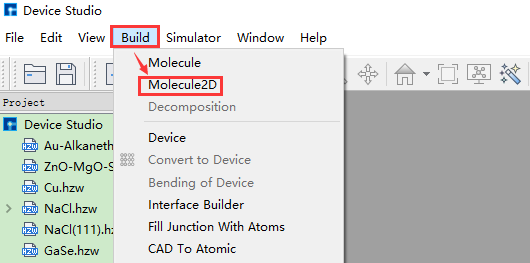
fig. 4.10 Pop-up 2D molecular modeling interface operation
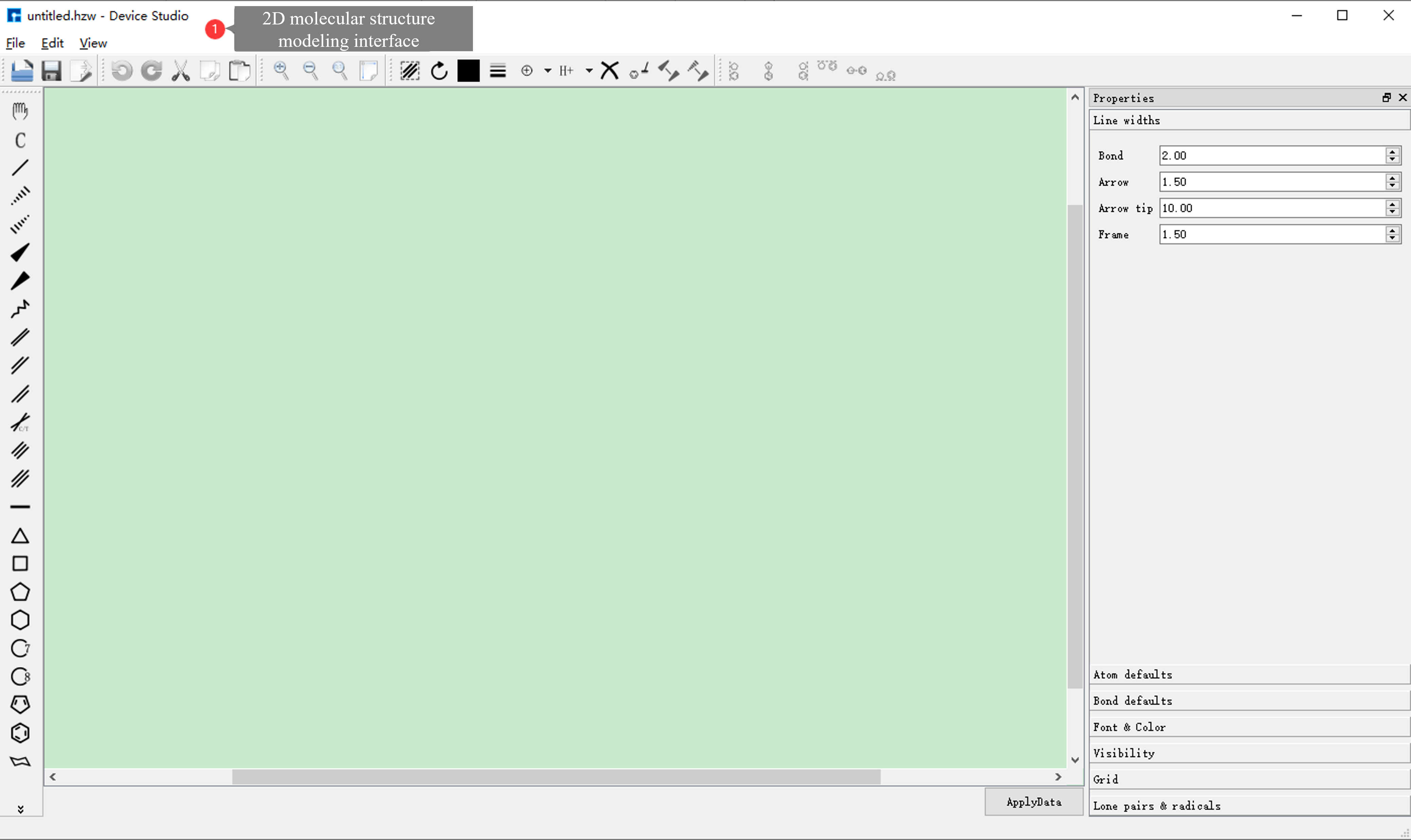
fig. 4.11 2D molecular modeling interface
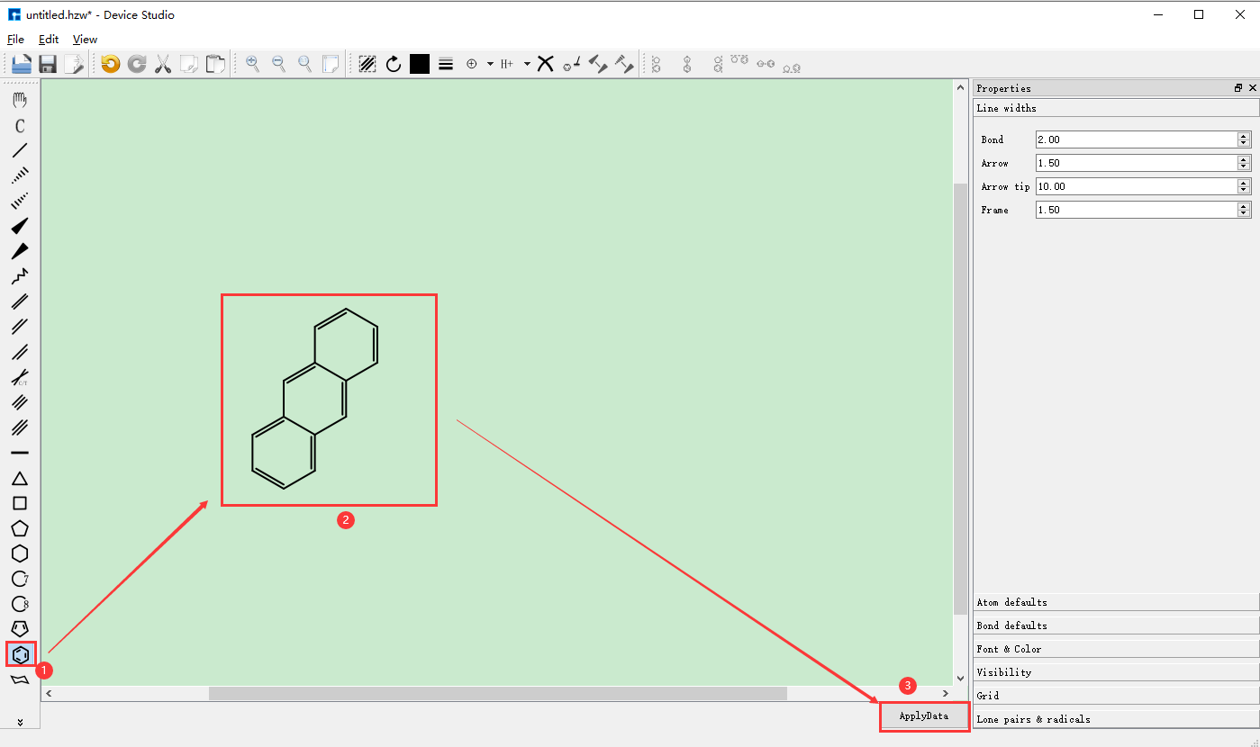
fig. 4.12 Building 2D molecular structure and converting to 3D molecular structure operation
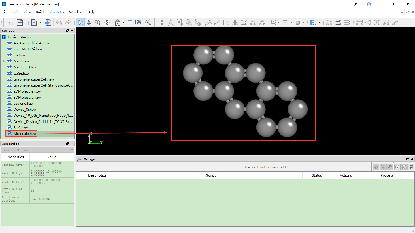
fig. 4.13 Device Studio interface after converting 2D molecular structure to 3D molecular structure
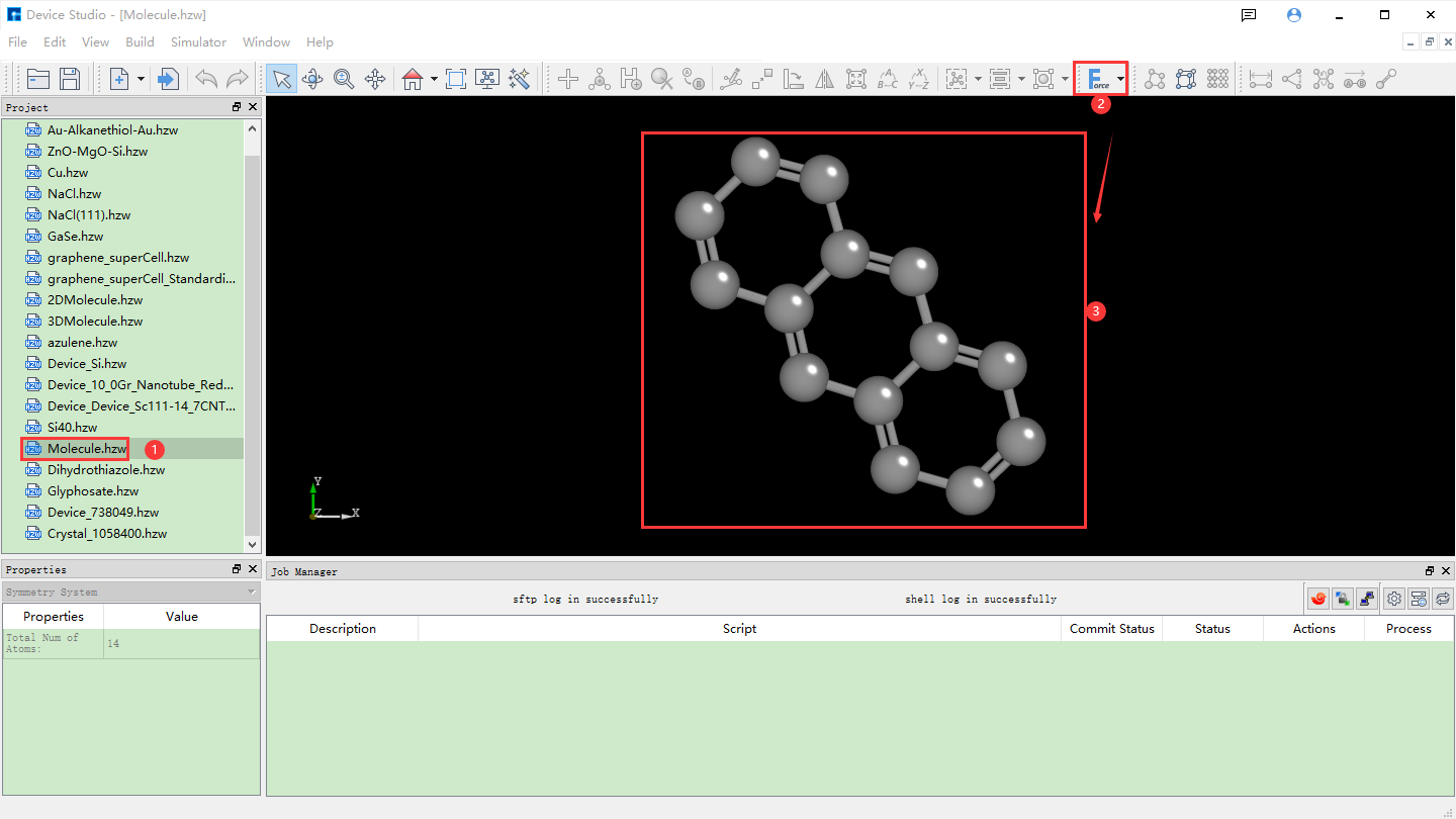
fig. 4.14 Optimizing converted 3D molecular structure operation
Note
The Minimize Structure labeled as (2) in fig. 4.14 is for structural optimization of molecular structures through molecular force field calculations, defaulting to MMFF94. You can select an appropriate force field for structural optimization by clicking the dropdown button.
Device Studio 2022A version adds the 3D Molecular Modeling function. Users can quickly and conveniently build 3D molecular structures through this function. Device Studio supports editing 3D molecular structures and can view detailed information about atomic coordinates and bonds between atoms. It can perform a series of operations on molecular structures such as bond adjustment, atomic angle adjustment, dihedral angle adjustment, adding hydrogen, translation, rotation, renaming, copying fragments, adding, deleting, and modifying. The operation interface for building 3D molecular structures in Device Studio is shown in fig. 4.15, fig. 4.16, fig. 4.17, fig. 4.18, and fig. 4.19.
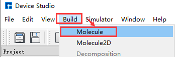
fig. 4.15 Pop-up 3D molecular modeling interface operation
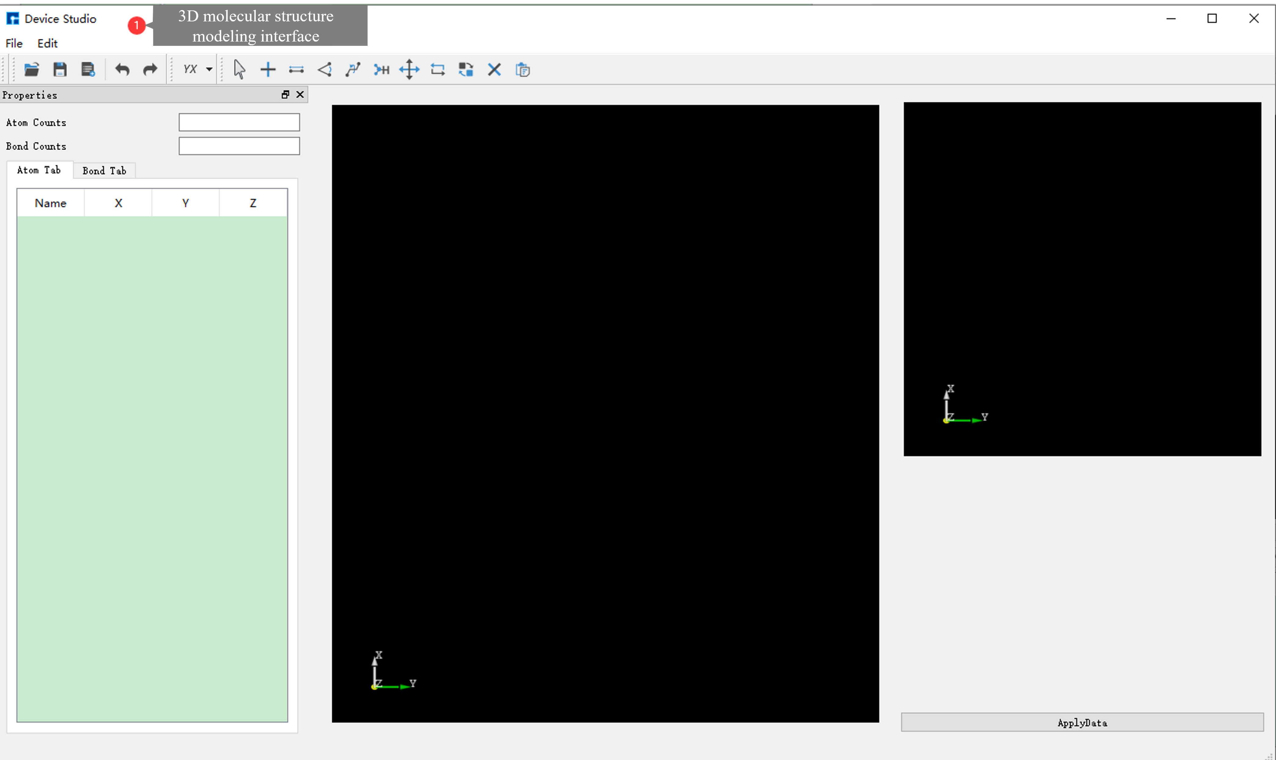
fig. 4.16 3D molecular modeling interface
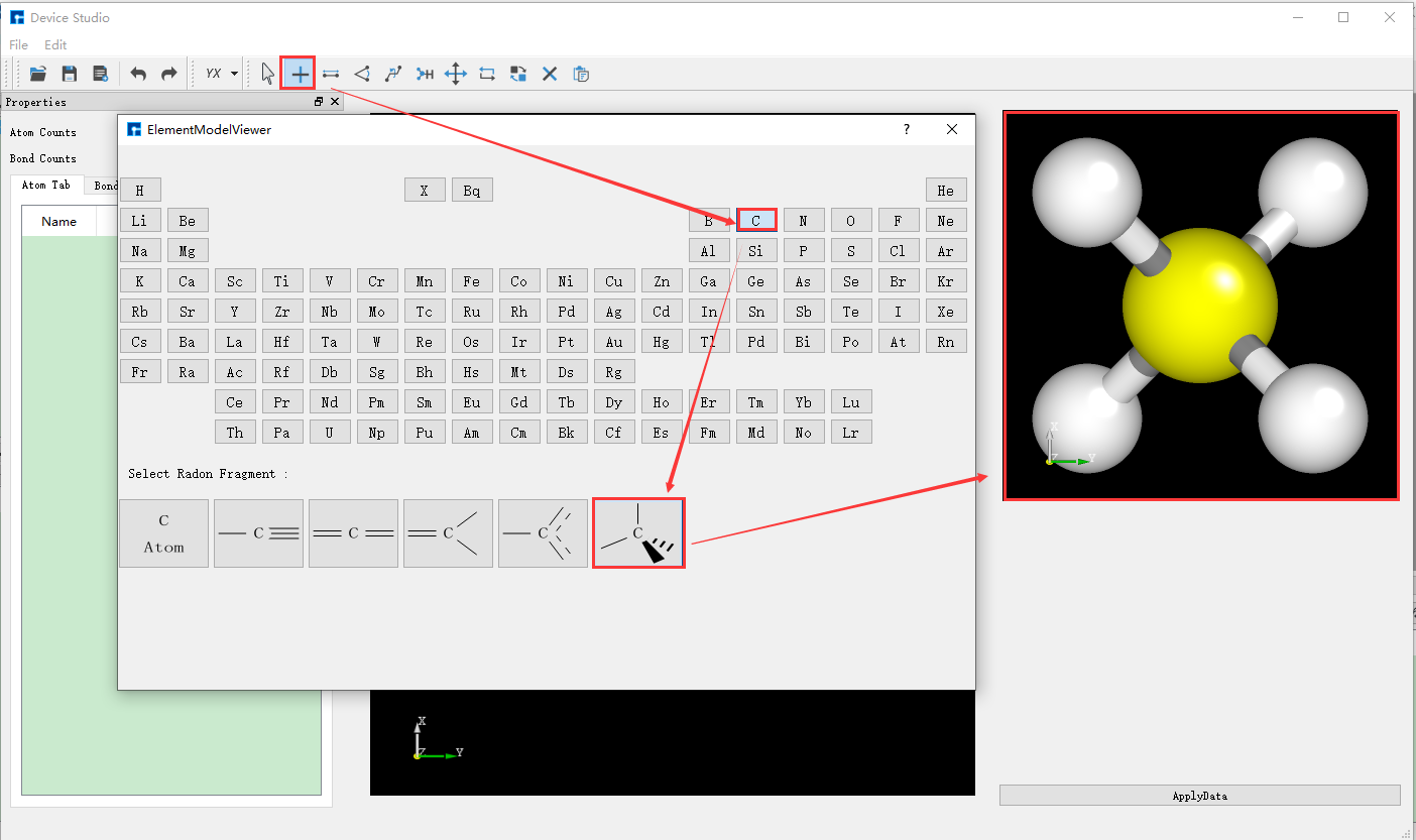
fig. 4.17 Building 3D molecular structure operation one
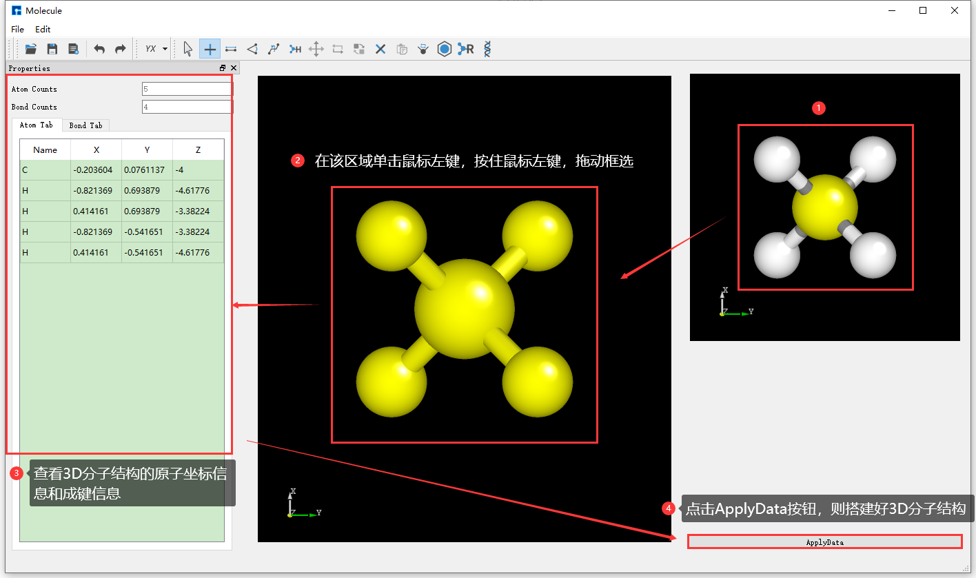
fig. 4.18 Building 3D molecular structure operation two
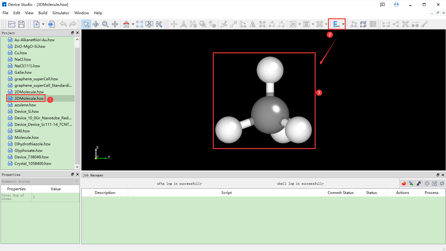
fig. 4.19 Optimizing built 3D molecular structure
For crystal modeling, users can first search whether the structure exists in the local database or online database. If it exists, import it directly; if not, they can build it themselves or import a structure and build upon it. Users can choose how to build the crystal structure according to their needs.
Taking the construction of NaCl crystal structure as an example, click Build → Crystal in the Device Studio graphical interface, and the interface for building crystal structure pops up as shown in fig. 4.20.
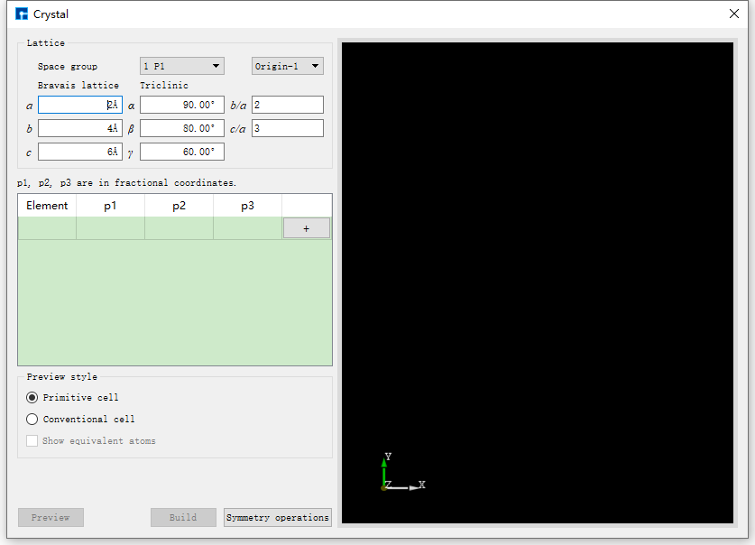
fig. 4.20 Crystal structure building interface
If you don’t know the space group information of the NaCl crystal, when building the NaCl crystal structure in the interface shown in fig. 4.20, you can follow the red box selection and arrow direction shown in fig. 4.21, fill in or select the corresponding information step by step, click the Preview button to preview the built structure in the right area of the interface. This step is mainly used to check whether the built structure is correct and whether it is the desired structure. Then click Build to build the NaCl crystal structure. The structure file is saved in the software’s project management area (Project Explorer), and you can view the 3D view of the structure in the 3D display area. Conversely, if you find that the built structure is incorrect during the preview process, you can rebuild it in the interface shown in fig. 4.20. During the structure building process, users can choose the Preview style in the interface according to their needs, that is, select Primitive cell or Conventional cell; choose whether to show equivalent position atoms, that is, whether to check Show equivalent atoms.
- The p1, p2, p3 values of the NaCl crystal structure are shown in the following table:
Element
p1
p2
p3
Na
0
0
0
Na
0.5
0.5
0
Na
0.5
0
0.5
Na
0
0.5
0.5
Cl
0.5
0
0
Cl
0
0.5
0
Cl
0
0
0.5
Cl
0.5
0.5
0.5
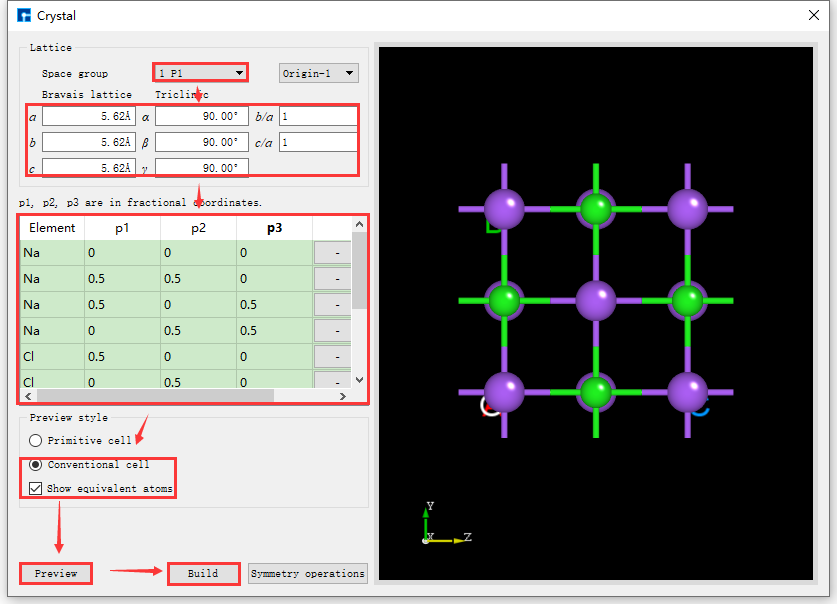
fig. 4.21 NaCl crystal structure building interface without space group information
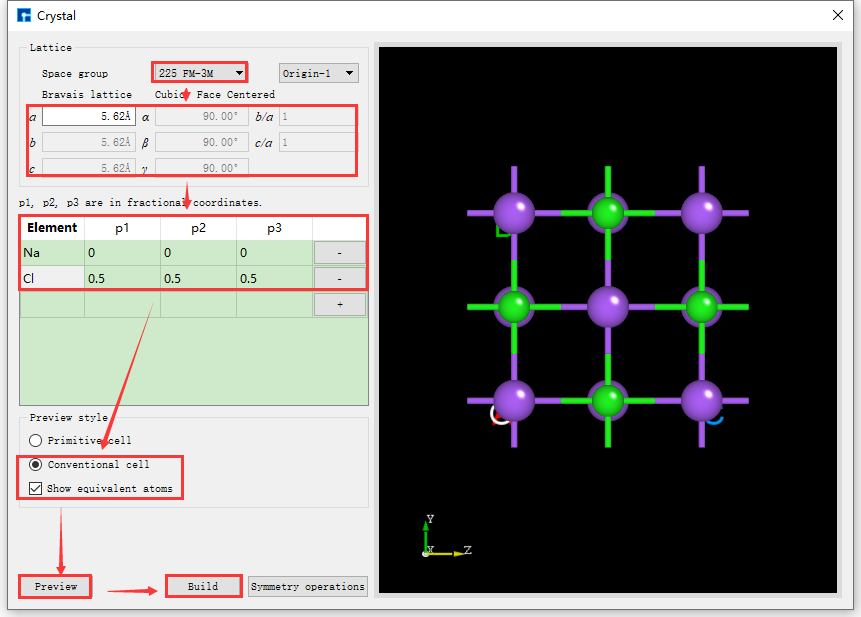
fig. 4.22 NaCl Crystal Structure Building Interface Based on Space Group Information
If the space group information of the structure is known, it can be built more conveniently and quickly. Device Studio supports the selection of 261 space groups (including 230 space groups and 31 extended subgroups). For example, the space group of NaCl crystal is 225 FM-3M. Knowing this information, when building the NaCl crystal in the interface shown in fig. 4.20, you can fill in the corresponding information as indicated by the red box and arrow in fig. 4.22. Other operations are consistent with those without knowing the space group information and will not be described in detail here. Comparing fig. 4.21 and fig. 4.22, it is clear that knowing the space group information can simplify the construction of the crystal structure.
Figures fig. 4.21 and fig. 4.22 both show the result of displaying equivalent atoms when building the NaCl crystal structure, i.e., with the Show equivalent atoms option checked. If this option is unchecked, the interface will appear as shown in fig. 4.23. Clicking the Build button in the interface will build the NaCl crystal structure. The structure file is saved in the software’s project management area, and a 3D view of the structure is displayed in the 3D display area. The interface after building the NaCl crystal structure is shown in fig. 4.24.
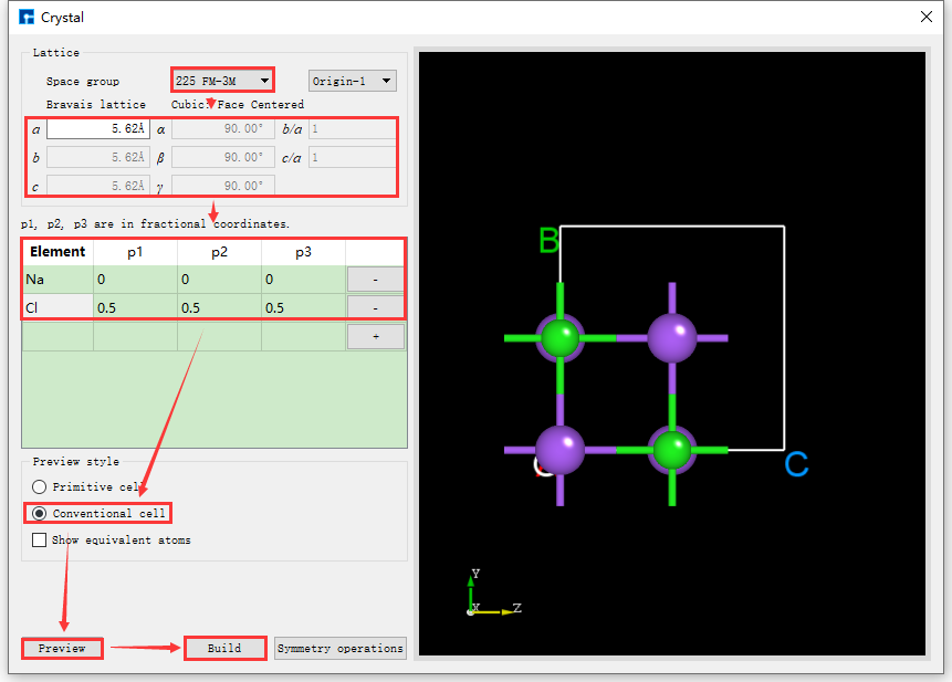
fig. 4.23 NaCl Crystal Structure Building Interface Without Equivalent Position Atoms Displayed
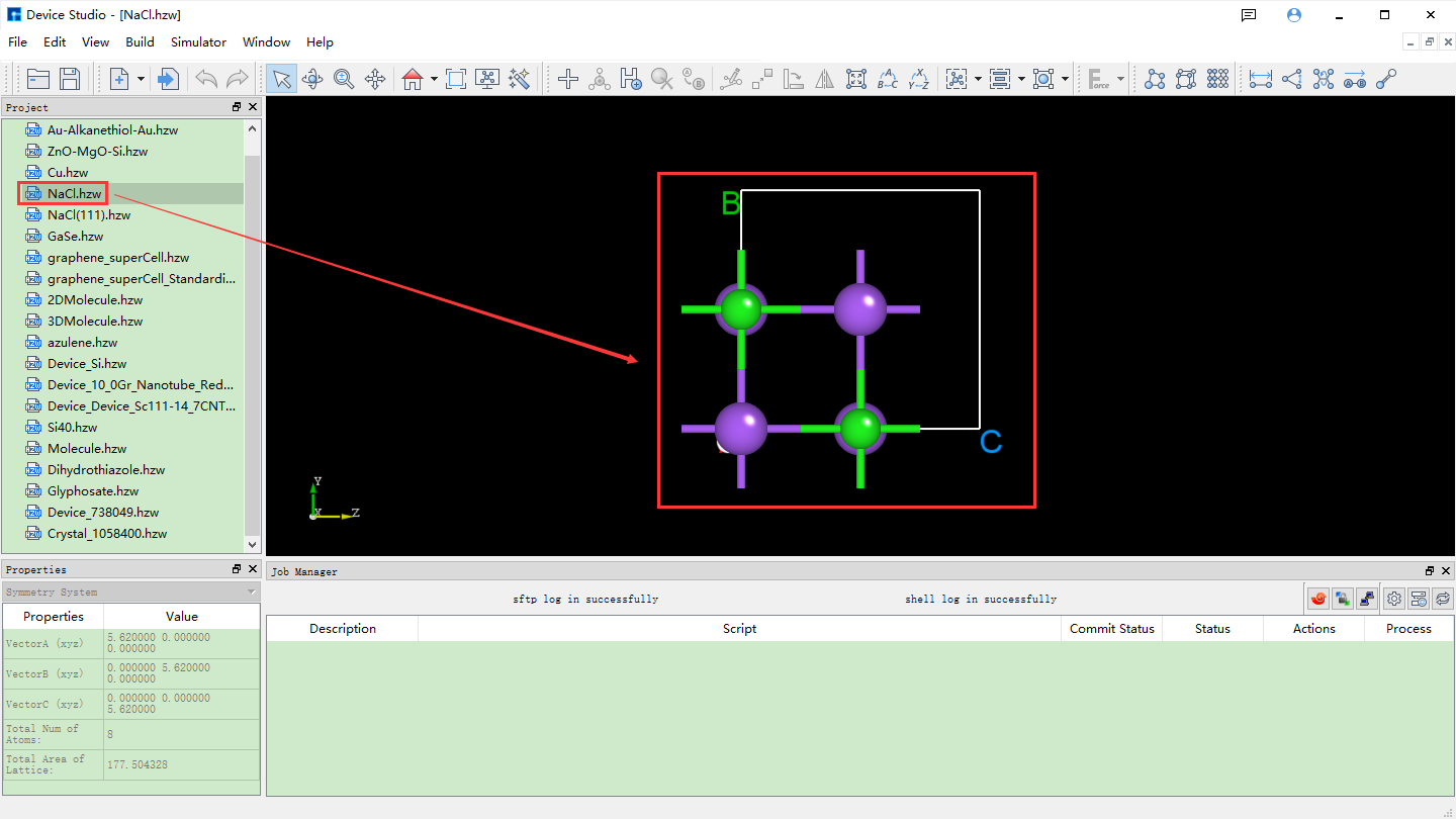
fig. 4.24 Device Studio Interface for Building NaCl Crystal Structure
Surface/Slab from Crystal Structure, this function is only available when a crystal structure exists. Taking the NaCl crystal structure built in the Crystal Modeling section as an example, to build a NaCl (1 1 1) crystal structure with a Thickness of 9.73 Å, click Build → Surface/Slab in the interface shown in fig. 4.24. The interface for building the surface/slab of the NaCl crystal structure will pop up as shown in fig. 4.25.
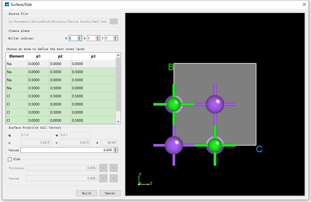
fig. 4.25 The interface for creating a slab/slice of the NaCl crystal structure
As shown in the red box and arrow in fig. 4.26, set the Miller index (1 1 1) in the interface shown in fig. 4.25. Select the Na (0.5000 0.5000 0.0000) atom as the starting atom for the slab in the dropdown table. Check the Slab box and click the + button after Thickness 5 times to set the Thickness to 9.73 Å. The structure can be previewed in the right panel. Click Build to build the 9.73 Å thick NaCl (1 1 1) crystal structure. The structure file is mounted in the Device Studio project management area, and the 3D view is displayed in the Device Studio 3D display area. The Device Studio interface after building the 9.73 Å thick NaCl (1 1 1) crystal structure is shown in fig. 4.27.
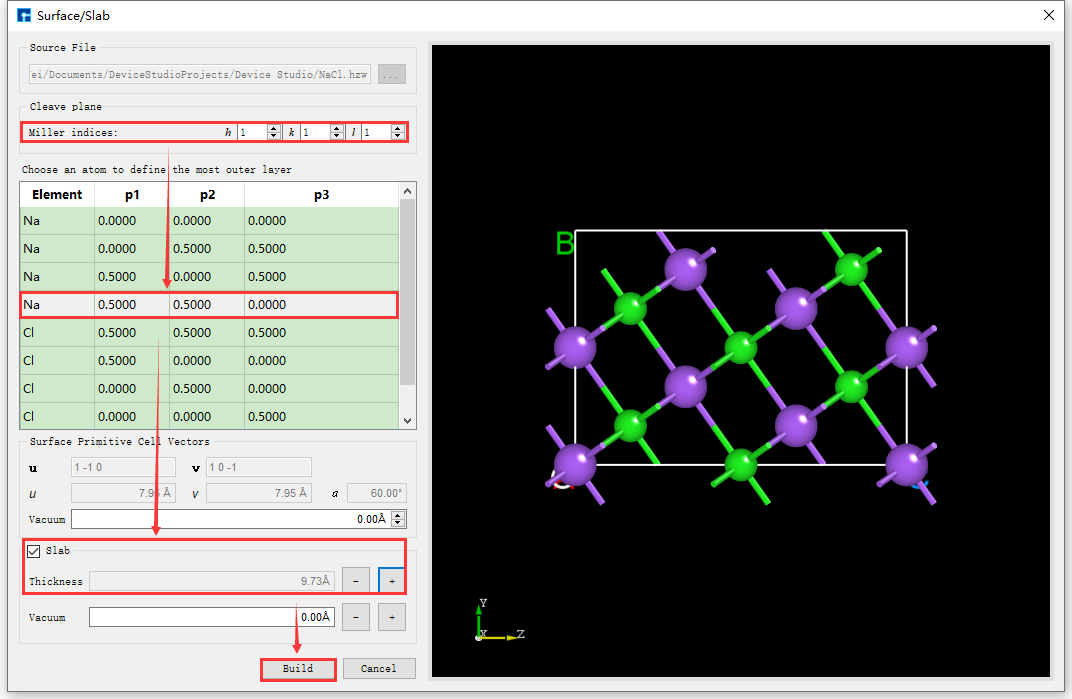
fig. 4.26 User interface for building a NaCl (1 1 1) crystal structure with a thickness of 9.73 Å.
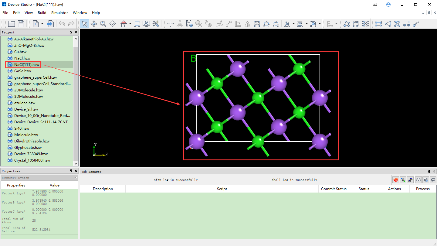
fig. 4.27 Set up the Device Studio interface for a NaCl (1 1 1) crystal structure with a Thickness of 9.73 Å.
After importing the Cu unit cell structure into Device Studio, the interface is shown as fig. 4.28. Click Build → Redefine Crystal in the interface to open the Cu unit cell structure crystal redefinition interface, as shown in fig. 4.29. Fill in the parameters according to the red boxed area in fig. 4.30. After filling in the parameters, click the Preview button to preview the supercell structure on the right side of the interface. Then, click the Build button to expand the Cu unit cell into a single cell. Simultaneously, the structure file Cu_Rede.hzw is mounted in the Device Studio project management area, and the 3D view of the structure is displayed in the Device Studio 3D display area, as shown in fig. 4.31.
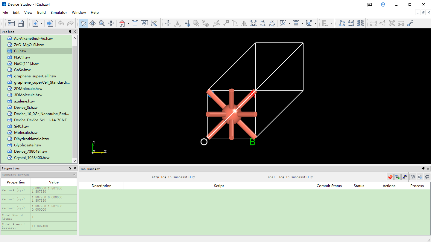
fig. 4.28 Device Studio interface after importing the Cu unit cell structure (Cu.hzw)
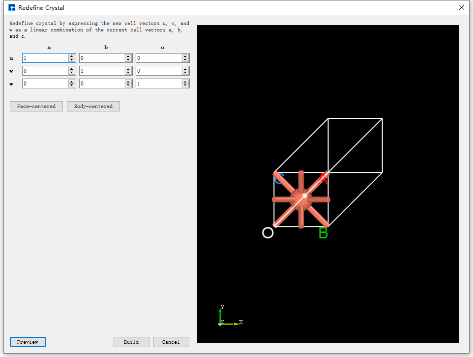
fig. 4.29 Cu Unit Cell Structure Redefinition Interface
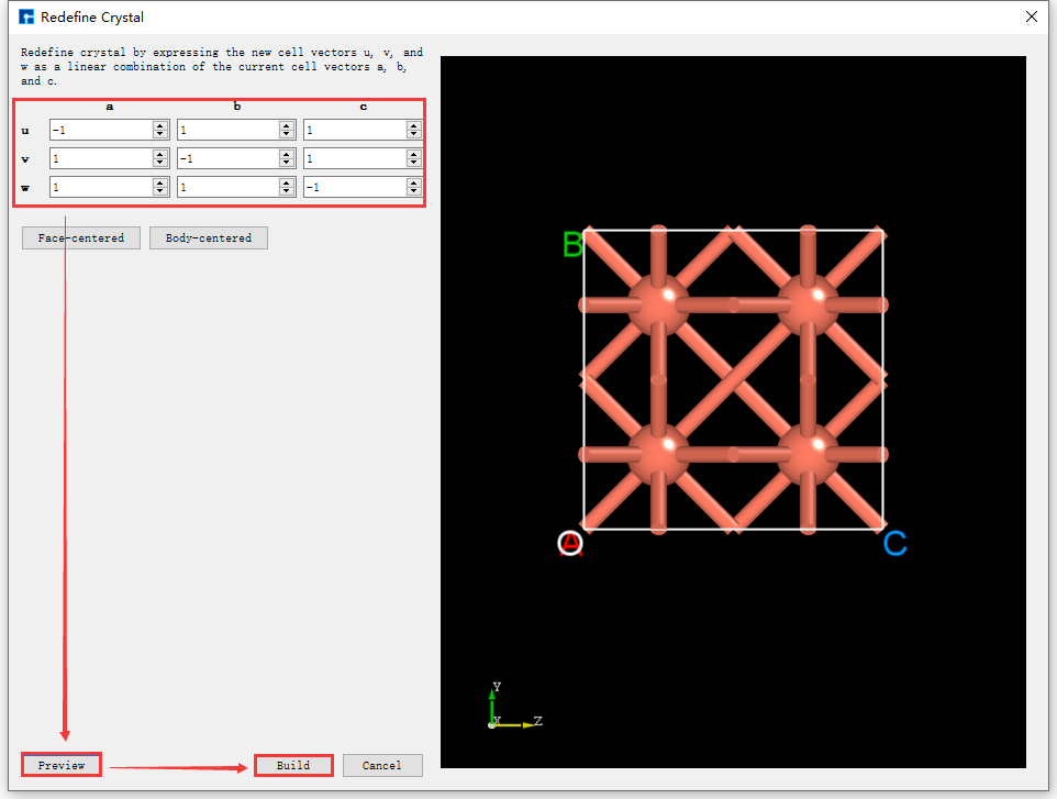
fig. 4.30 The interface for expanding the Cu unit cell structure into a supercell.
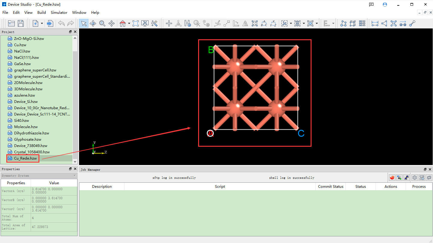
fig. 4.31 3D view of the Cu unit cell (Cu_Rede.hzw) in Device Studio
The supercell can be built from the unit cell by using the “Redefine Crystal” function in Device Studio. The operation is the same as expanding the Cu primitive cell to a unit cell. For example, to expand the Cu unit cell to a 4x4x4 supercell, click fig. 4.31 Build → Redefine Crystal. The “Redefine Crystal” interface will pop up, as shown in fig. 4.32. Follow the steps indicated by the red boxes and arrows in fig. 4.32. After clicking the Build button, the Cu unit cell will be expanded to a 4x4x4 supercell. The structure file Cu_Rede_Rede.hzw will be mounted in the project management area of Device Studio, and the 3D view of the structure will be displayed in the 3D display area of Device Studio, as shown in fig. 4.33.
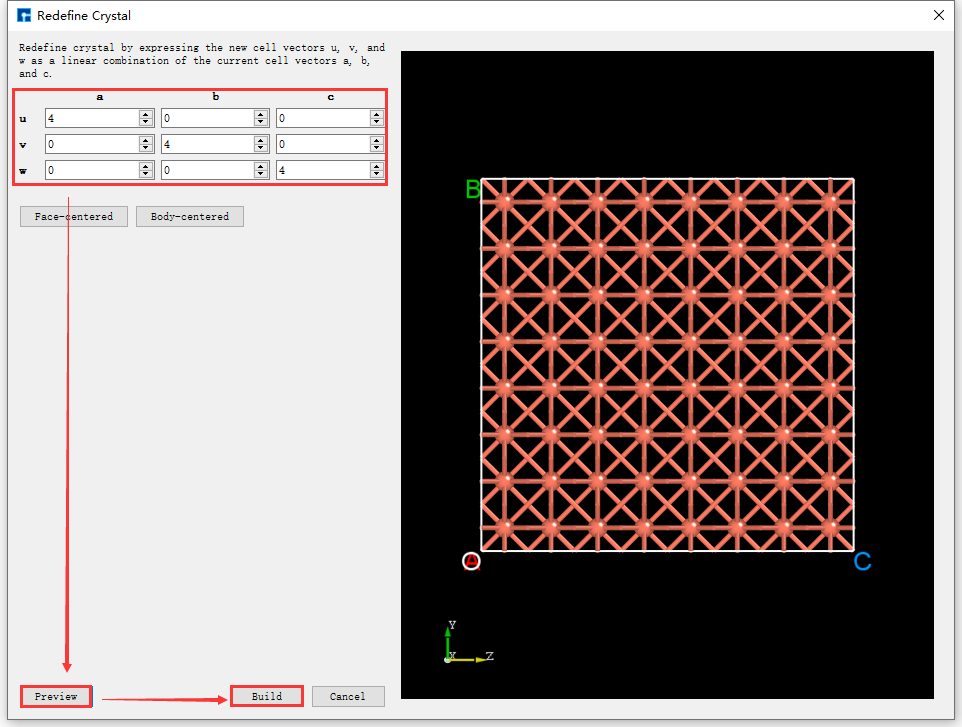
fig. 4.32 Interface for expanding the Cu unit cell to a 4x4x4 supercell
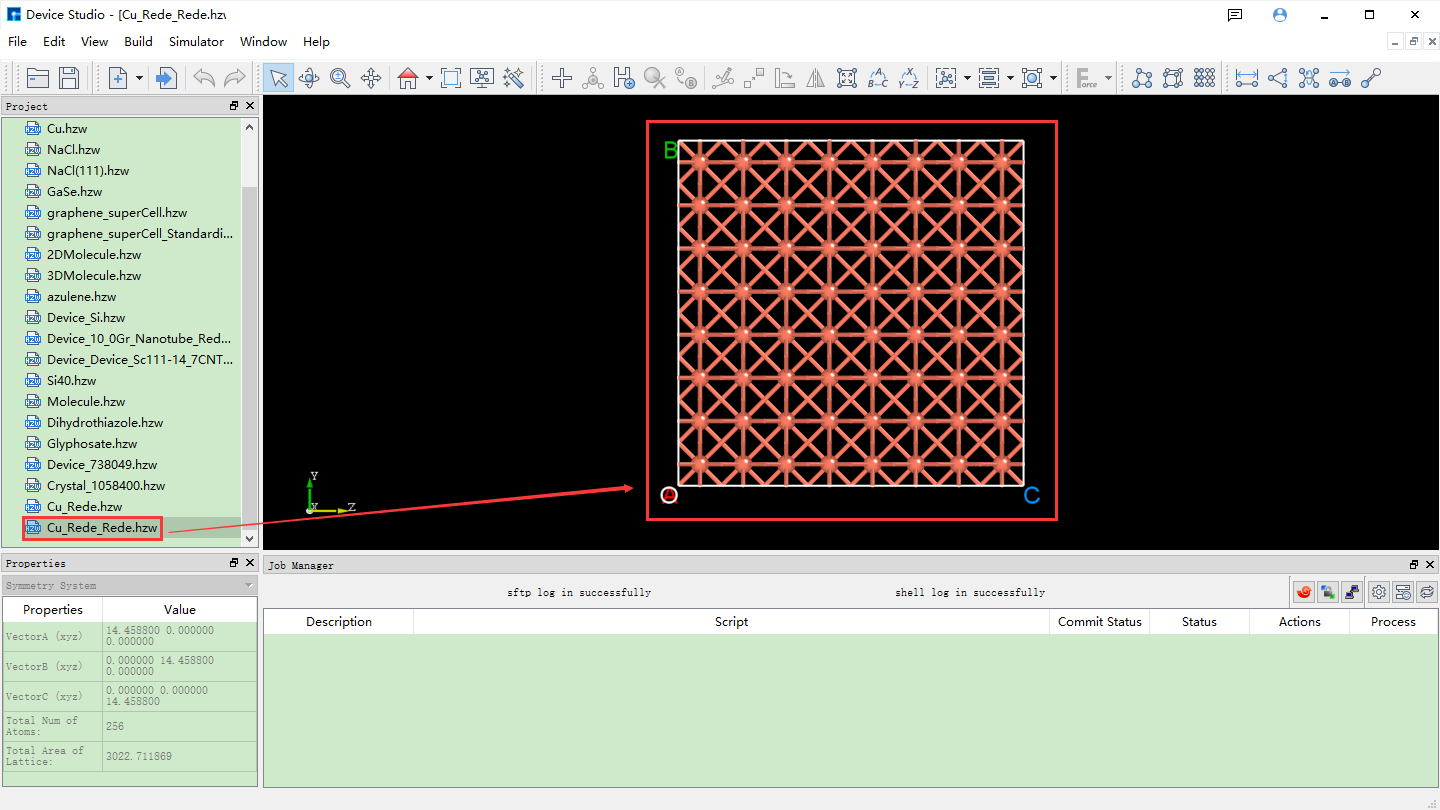
fig. 4.33 3D view of the Cu supercell (Cu_Rede_Rede.hzw) structure in Device Studio
Taking the construction of a gold-alkanethiol-gold (Au-Alkanethiol-Au) molecular device structure as an example, the following steps will detail the construction process.
4.3. Importing the Au Crystal Structure
*Import the Au crystal structure from the Device Studio local database, i.e., import the Au primitive cell. The import process is not described in detail here; users can refer to local_database_import_structure. The interface after importing the Au crystal structure is shown in fig. 4.34.
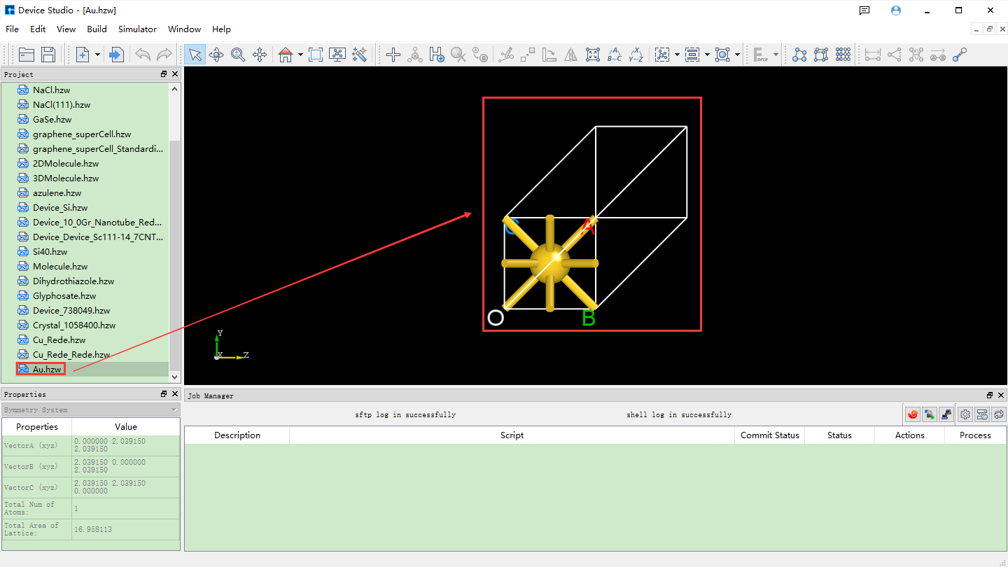
fig. 4.34 Interface after importing the Au crystal structure
4.4. Converting an Au primitive cell to an Au conventional cell
Click Build → Redefine Crystal in fig. 4.34, which will pop up the Redefine Crystal interface as shown in fig. 4.35. Click Face-centered → Preview in fig. 4.35, and the interface will change as shown in fig. 4.36. Users can preview the converted structure in the right area of fig. 4.36. After clicking Build, the Au primitive cell will be converted into an Au crystal cell. The structure file is saved in the software’s project management area (Project Explorer), and a 3D view of the structure can be seen in the 3D display area, as shown in fig. 4.37. Au.hzw in fig. 4.37 corresponds to the Au primitive cell, and Au_Rede.hzw corresponds to the Au crystal cell. Users can select the structure file according to their computational needs, right-click and select Rename to rename the structure file.
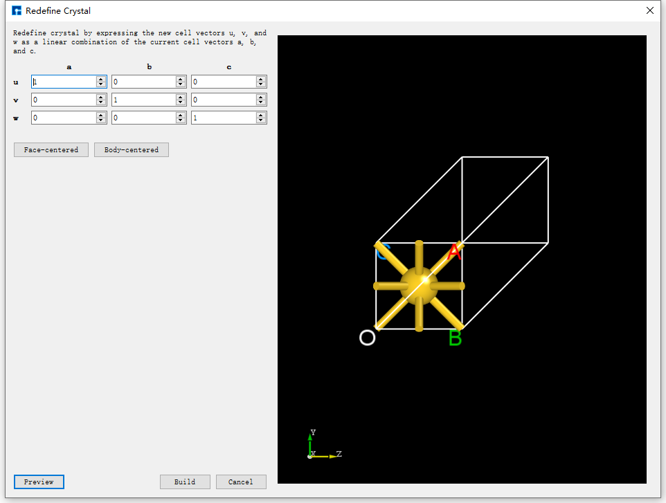
fig. 4.35 Redefine Crystal Interface for Au Unit Cell
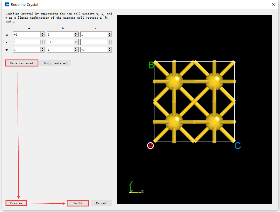
fig. 4.36 The operation interface for converting an Au unit cell to an Au crystal cell
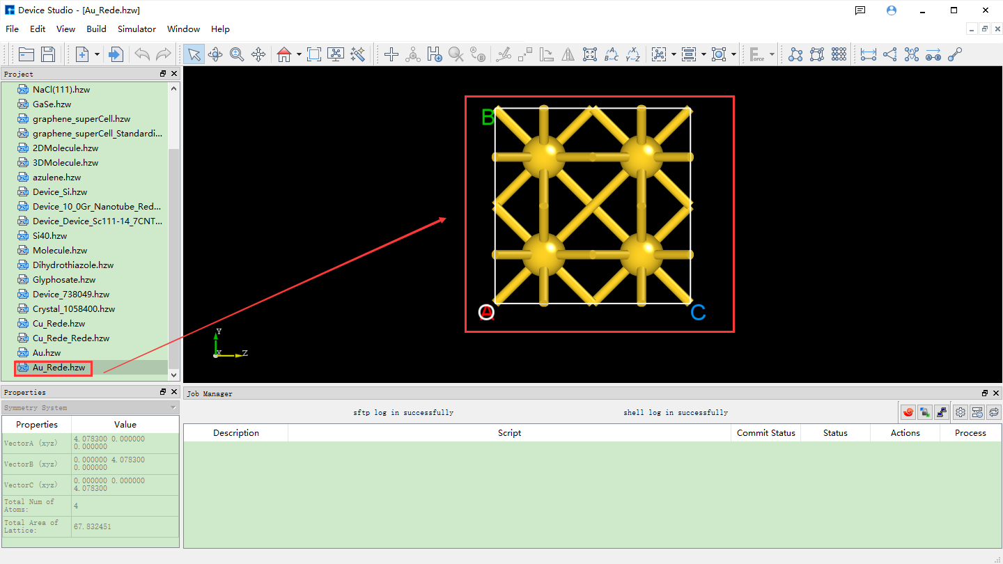
fig. 4.37 Interface after converting the Au primitive cell to the Au conventional cell
4.5. Converting an Au unit cell to an Au supercell
Convert the Au unit cell to a 2*2*4 supercell (referred to as: Au supercell). Click Build → Redefine Crystal in fig. 4.37 to open the Redefine Crystal interface. Modify the parameters as shown in the red box in fig. 4.38. Click Preview to preview the converted supercell structure. Clicking Build converts the Au unit cell into the Au supercell structure. The structure file is saved in the software’s project management area (Project Explorer), and a 3D view of the structure can be seen in the 3D display area, as shown in fig. 4.39. Au_Rede_Rede.hzw in fig. 4.39 corresponds to the Au supercell; users can rename this structure file according to their computational needs.
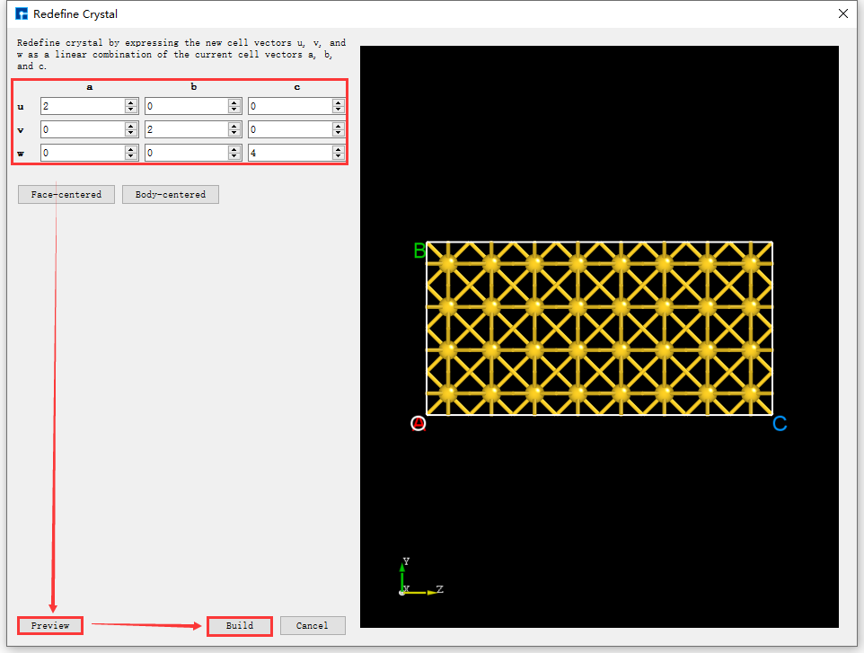
fig. 4.38 Operation interface for converting an Au unit cell to an Au supercell
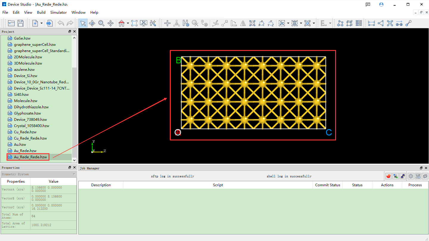
fig. 4.39 Interface after converting the Au unit cell to a Au supercell
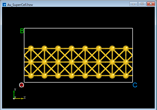
4.6. Removing Redundant Atoms and Operations in the Au Supercell
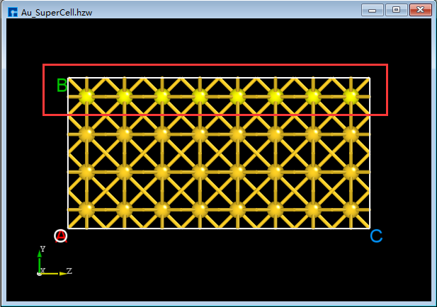
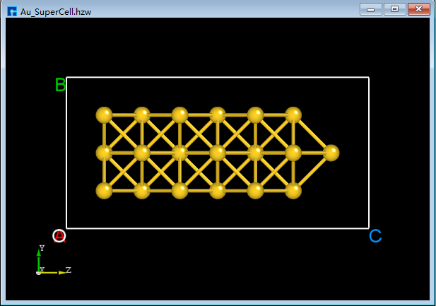
*Remove redundant atoms from the Au supercell and center the structure within the unit cell. To avoid accidentally deleting atoms and making them irretrievable, it is recommended to copy the Au supercell. Select the Au_Rede_Rede.hzw structure file → right-click → Copy. The CopyFile interface will appear, as shown in fig. 4.40. Users can rename the file according to their computational needs, such as Au_SuperCell, or directly use the default name. Then, click the OK button in the CopyFile interface. The Au_SuperCell.hzw structure file will be stored in the project management area. Double-click this structure file; its 3D view will be displayed as shown in BuildStructure_41 (a).
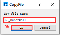
fig. 4.40 CopyFile Interface
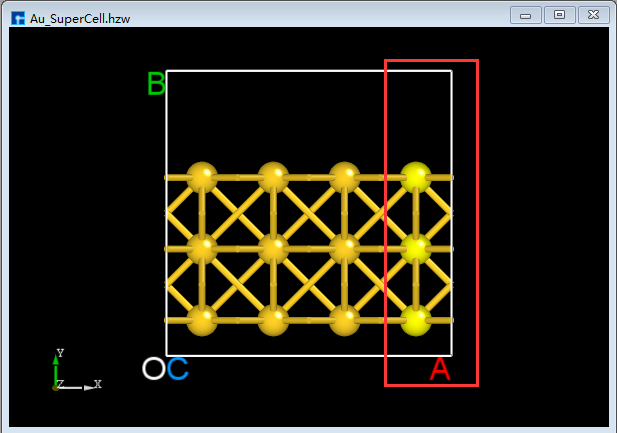
In the 3D display area, with the zy-plane view, mouse-select the area indicated by the red box in
BuildStructure_41(a), then click the Delete Atom icon in the toolbar or press the Delete key on the keyboard to delete the selected atoms. The result is shown inBuildStructure_42(b).Click the dropdown button to the right of the 3D Viewer zy View icon on the Toolbars and select xy View to switch from the zy-plane to the xy-plane, as shown in
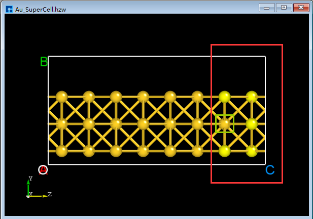
BuildStructure_43(c). Select the area within the red box inBuildStructure_43(c) using the mouse, and then click the Delete Atom icon on the Toolbars or press the Delete key to delete the selected atoms. After deletion, click the 3D Viewer zy View icon on the Toolbars to switch back to the zy-plane, as shown inBuildStructure_44(d). First, select the area within the red box inBuildStructure_44(d) using the mouse; second, hold down the Ctrl key and click the area within the green box inBuildStructure_44(d) with the mouse; finally, click the Delete Atom icon on the Toolbars or press the Delete key to delete the selected atoms. The result is shown inBuildStructure_45(e).In the case of
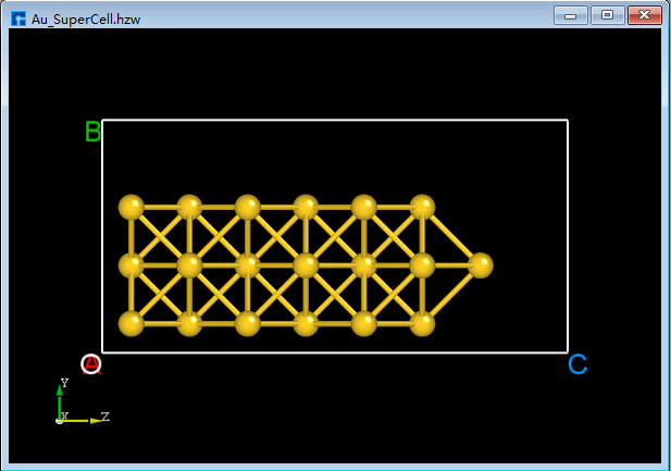
BuildStructure_45(e), clicking the Center icon on the Toolbars will center all atoms in the structure as a whole within the unit cell, as shown inBuildStructure_46(f). After completing the above series of operations, the structure fileAu_SuperCell.hzw(Au_SuperCell supercell) is obtained, and its 3D view is shown inBuildStructure_46(f).
note
Selected atoms are highlighted in yellow, allowing users to easily identify them.
|
|
|
|
|
|
4.7. Set X and Y axis directions to vacuum
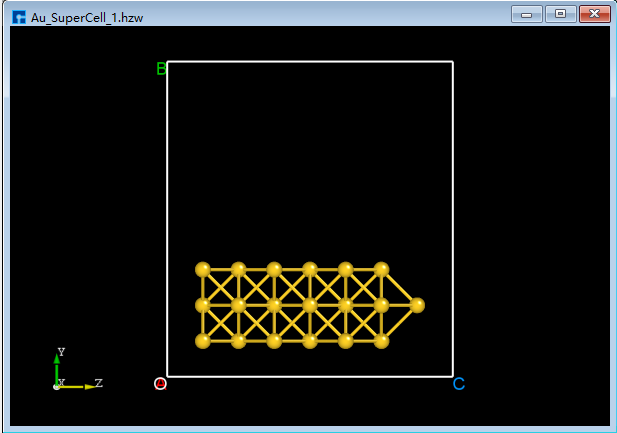
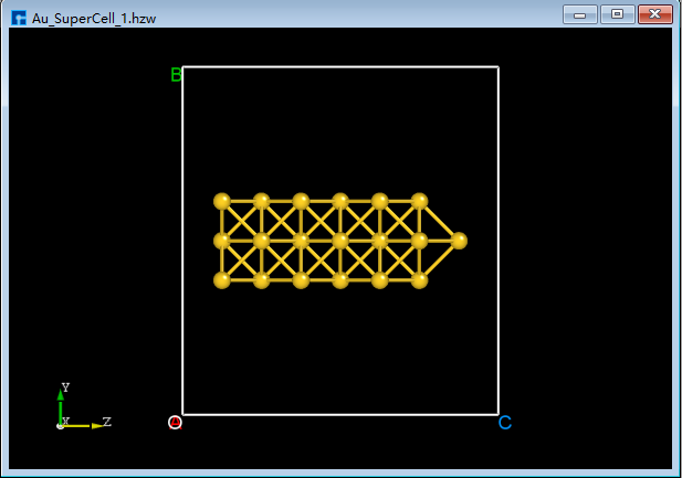
Set the X and Y axes of the Au_SuperCell supercell to vacuum. Duplicate the Au_SuperCell supercell and rename it Au_SuperCell_1. Double-click its structure file Au_SuperCell_1.hzw to display it in the 3D display area. Click the Convert to Crystal shortcut icon on the Toolbars to open the Convert to Crystal interface. Set the parameters as shown in the red box in fig. 4.41 → preview on the right side of the interface → Build. This will set the X and Y axes of the Au_SuperCell_1 supercell to vacuum, as shown in BuildStructure_48 (a). Click the Center shortcut icon on the Toolbars to center all atoms in the unit cell. After centering, the structure will appear as shown in BuildStructure_49 (b). After completing these steps, the structure file Au_SuperCell_1.hzw, representing the Au_SuperCell_1 supercell, will have a 3D view as shown in BuildStructure_49 (b).
note
Copying and renaming the structural files is for the convenience of this tutorial and to prevent irreversible errors after a series of operations. Users can decide whether to copy and rename them based on their modeling needs. Generally, for accidental deletions or misoperations, you can click the Undo shortcut icon on the Toolbars or press the Ctrl+Z shortcut to undo.
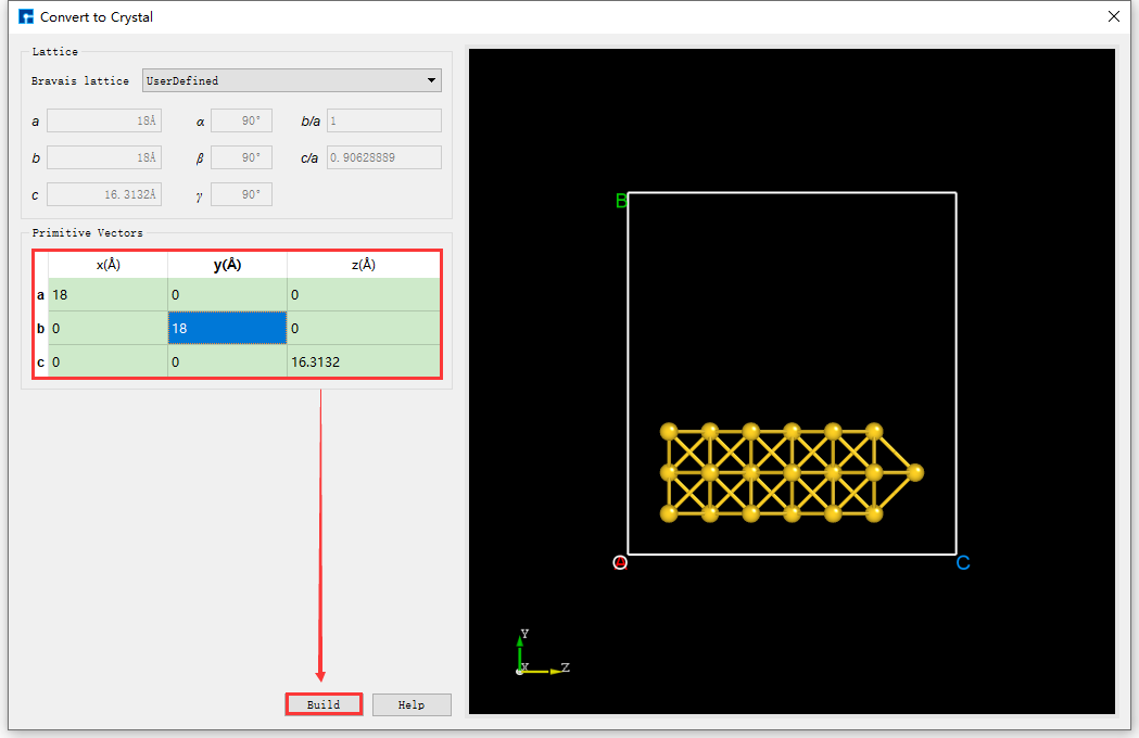
fig. 4.41 Convert to Crystal interface
note
After clicking the Build button in the fig. 4.41 interface, if the 3D view of the Au_SuperCell_1.hzw structure does not appear in the appropriate location in the 3D display area, the user can reset the 3D view to the appropriate location by clicking the 3D Viewer zy View shortcut icon on the Toolbars or by pressing the shortcut key Ctrl+R. The reset 3D view of the structure is shown in BuildStructure_49 (b). Users can use this method to reset the 3D view whenever it is not in the appropriate location in the 3D display area during the modeling process.
|
|
4.8. Mirror the structure and reset the lattice constants
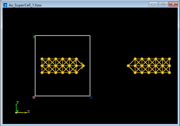
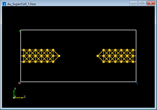
Mirror the selected atoms, reset the lattice constant, and center the structure. As shown in fig. 4.42, select all atoms → click the Mirror Atom shortcut icon → the Mirror interface pops up → set parameters → check Copy → click Apply. The structure will then be as shown in BuildStructure_52 (a). Based on BuildStructure_52 (a), click the Convert to Crystal shortcut icon. The Convert to Crystal interface will pop up, as shown in fig. 4.43. Set the parameters as shown in the red box in the figure. Preview the structure with the reset lattice constant on the right side of the interface. Click Build, then click the Center shortcut icon to center all atoms of the structure with the reset lattice constant in the unit cell. The centered structure is shown in BuildStructure_53 (b).
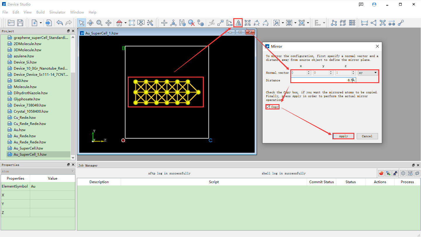
fig. 4.42 Au_SuperCell_1 Supercell Mirroring Operation Interface
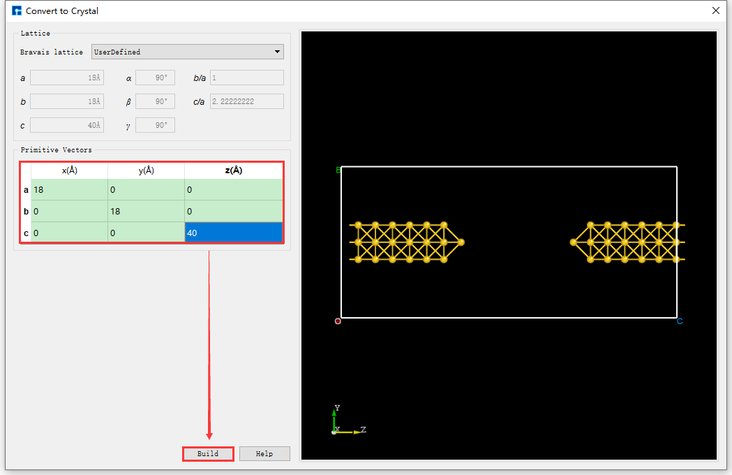
fig. 4.43 Au_SuperCell_1 Supercell Lattice Constant Resetting Operation Interface
|
|
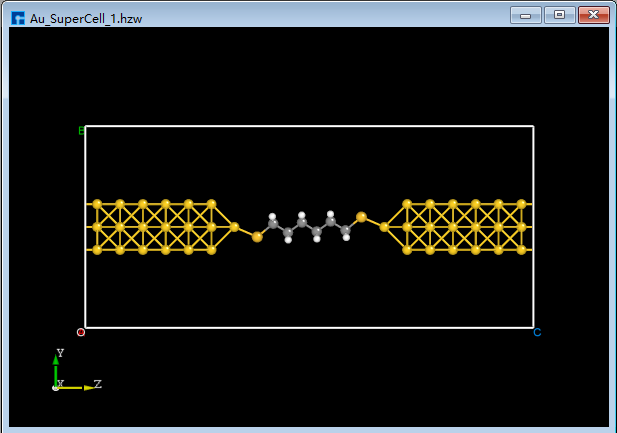
4.9. Setting up a Two-Port Device Structure
Import the alkanethiol molecule structure and copy it to the center of the Au_SuperCell_1 supercell structure. Then, build the two-port device structure.
Import the alkanethiol molecular structure as shown in fig. 4.44.
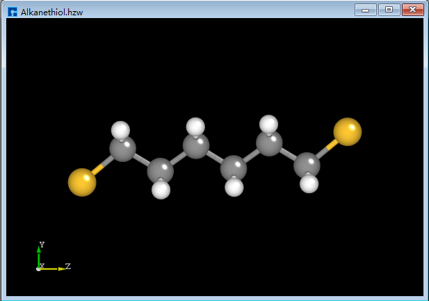
fig. 4.44 Alkanethiol molecule
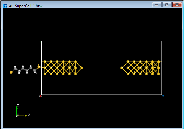
Double-click Au_SuperCell_1.hzw to open the Au_SuperCell_1 supercell structure. Box-select the alkanethiol molecule structure and press the shortcut key Ctrl+C to copy it. Click the left side of the interface in
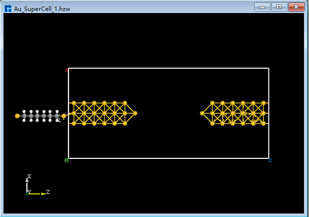
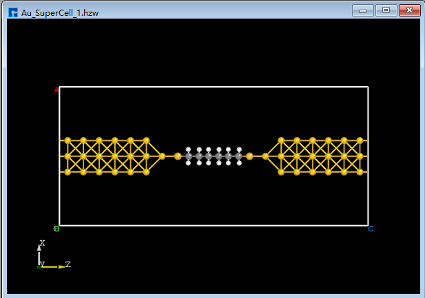
BuildStructure_53(b) and press the shortcut key Ctrl+V to paste the alkanethiol molecule structure into the Au_SuperCell_1 supercell structure, as shown inBuildStructure_55(a). To easily move the pasted alkanethiol molecule structure to the center of the Au_SuperCell_1 supercell structure, click the drop-down button to the right of the 3D Viewer zy View shortcut icon and select ZX zx View to switch from the zy plane to the zx plane, as shown inBuildStructure_56(b). Select the alkanethiol molecule structure and click the Center shortcut icon to move the alkanethiol molecule structure to the center of the Au_SuperCell_1 supercell structure, as shown inBuildStructure_57(c). Click the 3D Viewer zy View shortcut icon to switch back to the zy plane, as shown inBuildStructure_58(d).
|
|
|
|
|
|
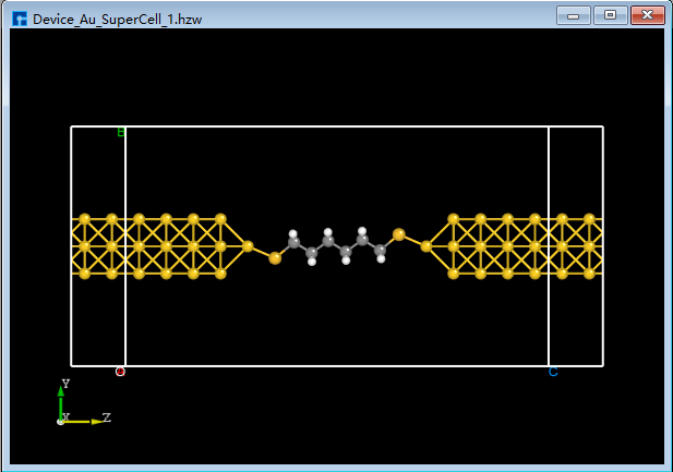
Click the Convert to Device shortcut icon. The Convert to Device interface will pop up, as shown in fig. 4.45. Select the parts in the red boxes, then click Preview to preview the two-port device structure on the right side of the interface. Clicking Build will generate the two-port device structure
Device_Au_SuperCell_1.hzw, as shown inBuildStructure_59(e).
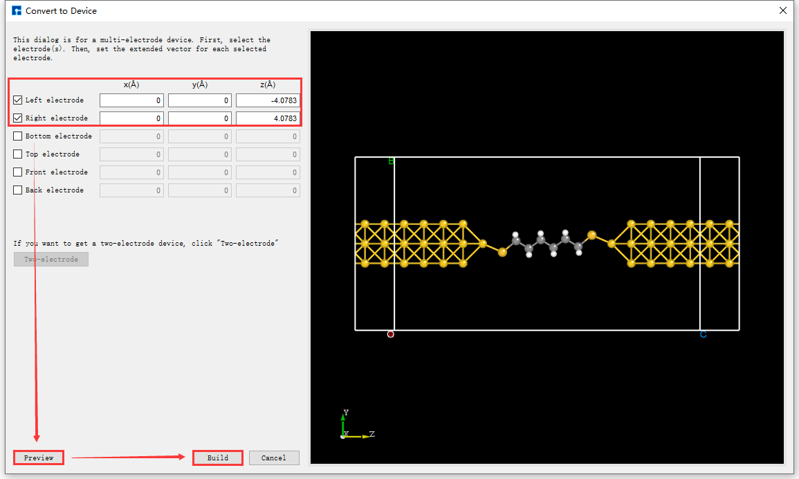
fig. 4.45 Convert to Device Interface
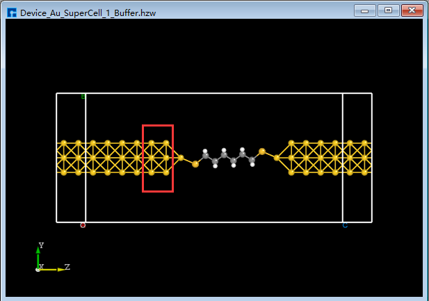
4.10. Adding a Buffer Layer to the Device Structure
Users can choose whether to add a buffer layer to the built two-port device structure based on computational needs; there is no mandatory requirement. For example, to add a buffer layer to the Device_Au_SuperCell_1.hzw device structure near the electrode along the transport direction (Z-axis), using an atom-layer incremental method, double-click to open the device structure → click Simulator → Nanodcal → Add Buffer in the software menu bar. The Add Buffer interface, as shown in fig. 4.46, will appear. Click the + button twice after Left. A preview of the buffer layer added to the left side of the device along the transport direction will be shown on the right side of the interface. Clicking Build will generate the two-port device structure with the added buffer layer, Device_Au_SuperCell_1_Buffer.hzw, as shown in BuildStructure_60 (f).
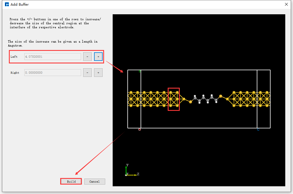
fig. 4.46 Add Buffer Interface
note
The addition of buffer layers to the device structure described above is merely an example; users can decide whether to add buffer layers near both ends of the electrodes and how many layers to add, based on their computational needs.
For a built structure, such as the two-port device structure Device_Au_SuperCell_1_Buffer.hzw, to export this structure file, double-click to open the structure file → click File → Export in the software to bring up the export interface. Users can select the storage location, name the structure file (or use the default name), and choose the storage format as needed.